Not really needed, yet I wanted to make/design something. I also wanted to try to build something with an ESP8266 (without development board). I still had some SMD components from my previous build: P1 to Ethernet
So I thought, why not a wireless version?
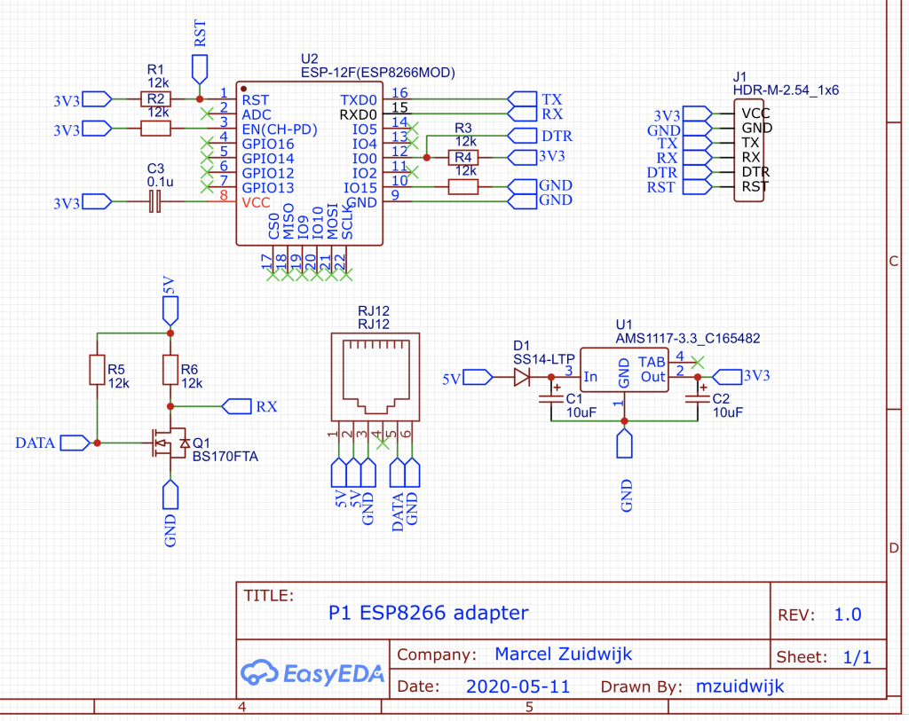
I started with the same inverter and a bare ESP8266-12F which I had laying around for several years. Looked up the minimal wiring for the esp and how to be able to flash it with firmware: esp-link.
After placing all the components on the sheet and wiring it up according to my idea, it looked something like this:
Spoiler alert: do you see my design flaw?
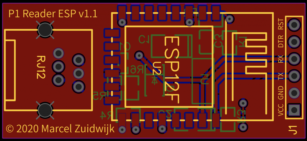
After rotating and routing for like a hour, I got the design that was as compact as it could get. The RJ12 header and the esp are the two biggest components. Everything else is on the back:
Two weeks later
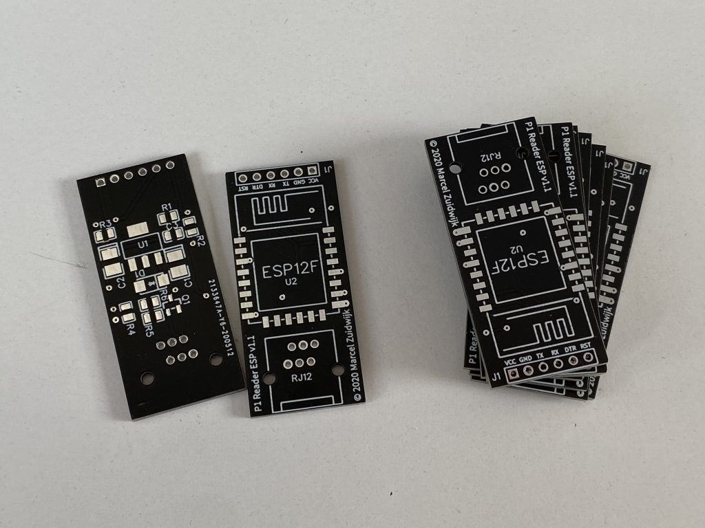
After about two weeks the prints arrived by mail. And again, those black PCB’s are damned sexy 😍
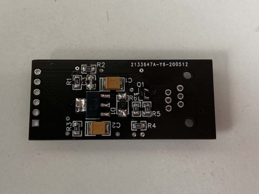
Soldering a SOT-23 (Q1) is quite the challenge. It’s possible, once you’ve got the right tactic. Everything else is easy:
Spoiler: do you see the design flaw now (if you didn’t saw it previously?)
Even the ESP8266 is easy to solder. Align it with one corner. Place a drop of solder and than fine tuning/placing the opposite corner. Once fixed, solder all the other pads:
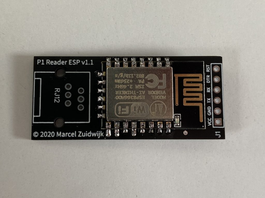
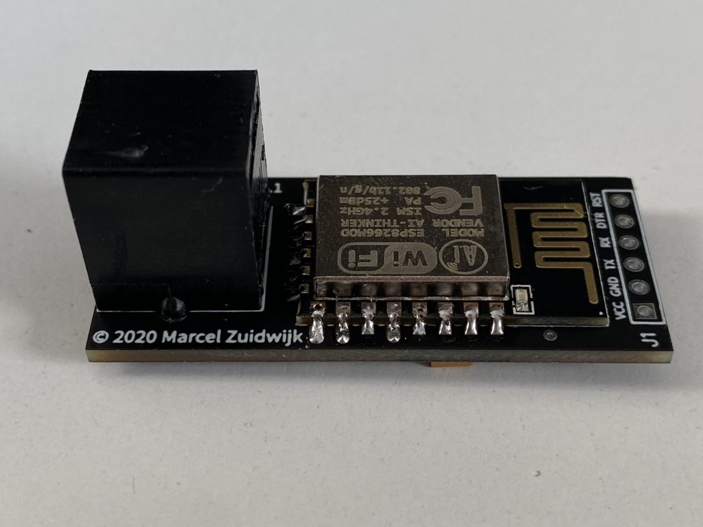
The end result is gorgeous!! This PCB is only 45x20mm small and completely powered by the P1 connector of the electricity meter.
Flashing the ESP8266
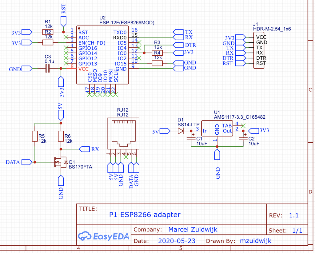
Then the moment I figured out there was a flaw in my design. Connecting it to my USB-Serial adapter, the led didn’t flashed. So troubleshooting began. Follow the traces and see if all the ground and vcc were right. And it didn’t, only 0.79 volt on the vcc instead of 3.3.
I followed every step to see where it dropped. And I saw that it dropped after the small capacitor. I looked it up in my design and guess what…? That capacitor should have been plaved between the vcc and gnd. And not in serie as it is in my design. #facepalm
So I removed the small capacitor, as it isn’t really needed. There are two other larger capacitors: C1 and C2. So I shorted the C3 pad on the PCB and after that fix I could flash the ESP with esp-link firmware.
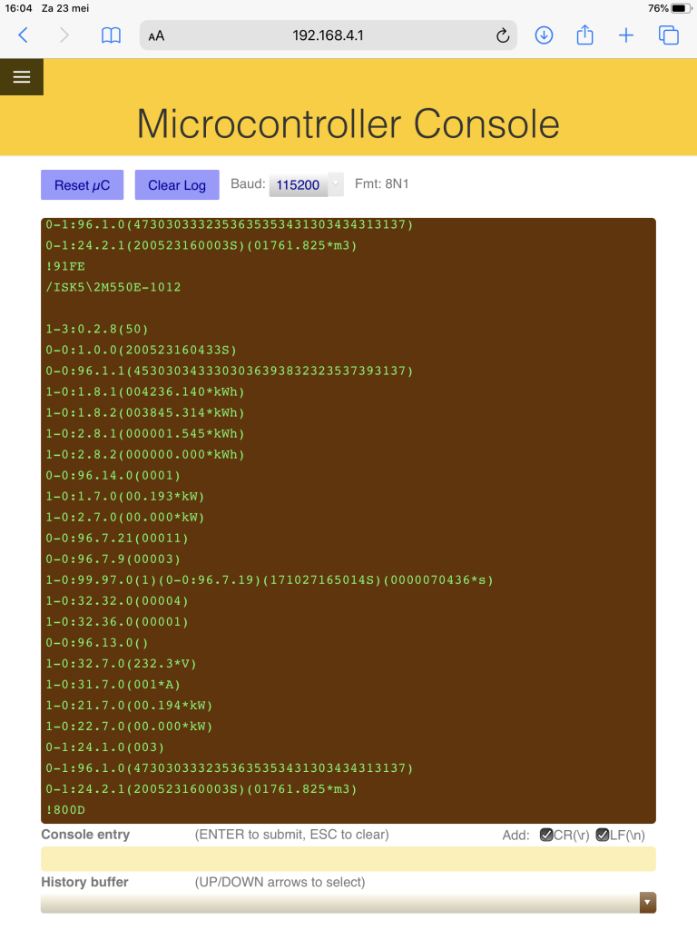
After flashing the firmware, I hooked it up to the P1 port and voila! It worked:
All it needs is to configure the right wireless network and it’s ready to go!
Thomas Buyukkilic
Hi Marcel, I was thinking of a similar solution, but then I saw your design/progress, looks good!
I was wondering if it would be possible to have a even smaller footprint:
– Remove the female RJ12 port and replace it with a Dupont 6-pin connector, RJ12 to dupont cables do exist (https://www.tinytronics.nl/shop/nl/kabels-en-connectoren/kabels-en-adapters/ethernet-en-telefoon/rj12-naar-6-pins-dupont-jumper-adapter)
– Remove USB port, allow the ESP8266 chip to be “clicked in” (just like those dev boards), or provide another Dupont connector to usb-c?
Would that be possible?
Marcel
I totally missed your message! But yeah that is possible. It will onle make it smaller in height if you rotate the connector to a 90º angle but you still need to place that cable connector. I’ve tried many things, as you only need 4 wires (data, enable, ground & 5v). At the end, it would make it way more costly that’s not worth the few mm gain.